
Optical Transceiver QSFP 100g LR4 10km RoHS Compliant


Short Description:
Functional Description Optical Transceiver QSFP 100G LR4 10km , a high-performance optical module engineered for long-haul data center and metro network connectivity. This hot-pluggable transceiver is fully compliant with the IEEE 802.3ba 40GBASE-ER4 standard and the QSFP MSA, ensuring seamless integration with your existing switches and routers. The module …Description
Specification
Application
Order
Downloads/FAQ
Product Tags
Reviews
Description
Functional Description
Optical Transceiver QSFP 100G LR4 10km , a high-performance optical module engineered for long-haul data center and metro network connectivity. This hot-pluggable transceiver is fully compliant with the IEEE 802.3ba 40GBASE-ER4 standard and the QSFP MSA, ensuring seamless integration with your existing switches and routers.
The module utilizes Coarse Wavelength Division Multiplexing (CWDM) technology, integrating four distributed feedback (DFB) lasers and a multiplexer to deliver a robust 40Gbps connection over a single duplex LC strand of single-mode fiber (SMF). With a reach of up to 40 kilometers, it provides a reliable, high-bandwidth solution for demanding applications like rack-to-rack interconnects, metropolitan area networks, and core switching. Its design incorporates an avalanche photodiode (APD) receiver for enhanced sensitivity, ensuring signal integrity over extended distances.
Optical Transceiver QSFP 100g LR4 10km Features
Duplex LC Receptacle Optical Interface: Offers stable and high-performance optical data transmission with easy connectivity.
Single +3.3V Power Supply: Simplifies power requirements while maintaining efficient performance.
Hot-Pluggable QSFP28 MSA Form Factor: Enables easy installation and upgrades without disrupting operations.
4x25G Electrical Serial Interface: Supports high-speed data transfer, delivering up to 100Gbps.
Compliant with 4x28G CEI-28G-VSR: Ensures compatibility with advanced high-speed signaling protocols.
Cooled 4x25Gb/s LAN WDM EML TOSA: Uses four electric-absorption modulated lasers (EMLs) at precise wavelengths for optimal signal integrity.
4x25Gb/s PIN ROSA Receiver: Provides high-sensitivity reception of optical signals for efficient data recovery.
Low Power Dissipation (Max: 6W): Designed for energy-efficient operation without compromising performance.
Built-in Digital Diagnostic Function: Enables real-time monitoring of module status for improved reliability and maintenance.
Applications
- 100GBASE-LR4
- Infiniband QDR and DDR interconnects
- 100G Datacom connections
Standards
- Compliant with IEEE 802.3ba
- Compliant with QSFP28 MSA hardware specifications
- Compliant with RoHS
Functional Diagram
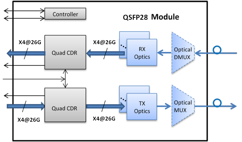
Absolute Maximum Ratings
| Parameter | Symbol | Min. | Max. | Unit | Note |
| Supply Voltage | Vcc | -0.5 | 3.6 | V | |
| Storage Temperature | TS | -40 | 85 | °C | |
| Relative Humidity | RH | 0 | 85 | % | |
| Rx Damage Threshold,per Lane | PRdmg | 5.5 | dBm |
Note: Stress in excess of the maximum absolute ratings can cause permanent damage to the transceiver.
Recommended Operating Conditions
| Parameter | Symbol | Min. | Typ | Max. | Unit | Note |
| Data Rate | DR | 103.1 | Gb/s | |||
| Supply Voltage | Vcc | 3.14 | 3.3 | 3.47 | V | |
| Supply Current | Icc | 1.8 | A | |||
| Operating Case Temp. | Tc | 0 | 70 | °C |
Electrical Characteristics (Top=0~70℃, Vcc=3.14~3.47V)
(Tested under recommended operating conditions,unless otherwise noted)
| Optical Transceiver QSFP 100g LR4 10km Parameter | Symbol | Min | Typ | Max | Unit | Notes | ||||
| Transmitter | ||||||||||
| Signaling rate per lane | DRPL | 25.78125 ± 100 ppm | Gb/s | |||||||
| Differential input return loss (min) | RLd(f) | 9.5 – 0.37f, 0.01≤f<8
4.75 – 7.4log10(f/14), 8 ≤f<19 |
dB | |||||||
| Differential to common mode input
return loss (min) |
RLdc(f) | 22-20(f/25.78), 0.01≤f<12.89
15-6(f/25.78), 12.89≤f<19
|
dB | |||||||
| Differential termination mismatch | Tm | 10 | % | |||||||
| Eye width | Ew | 0.46 | UI | |||||||
| Applied pk-pk sinusoidal jitter | Ppj | Per IEEE 802.3bm | ||||||||
| Eye height | Eh | 95 | mV | |||||||
| DC common mode voltage | DCv | -350 | 2850 | mV | ||||||
| Optical Transceiver QSFP 100g LR4 10km Receiver | ||||||||||
| Signaling rate per lane | DRPL | 25.78125 ± 100 ppm | Gb/s | |||||||
| Differential data output swing | Vout,pp | 400 | 800 | mV | ||||||
| Eye width | Ew | 0.57 | UI | |||||||
| Vertical eye closure | 5.5 | dB | ||||||||
| Differential output return loss (min) | RLd(f) | 9.5 – 0.37f, 0.01≤f<8
4.75 – 7.4log10(f/14), 8 ≤f<19
|
dB | |||||||
| Common to differential mode conver- sion return loss (min)
|
RLdc(f) | 22-20(f/25.78), 0.01≤f<12.89
15-6(f/25.78), 12.89≤f<19
|
dB | |||||||
| Differential termination mismatch | Tm | 10 | % | |||||||
| Transition time, 20% to 80% | Tr,Tf | 12 | ps | |||||||
Notes:
1.20%~80%
Optical Characteristics (Top=0~70℃, Vcc=3.14~3.47V)
(Tested under recommended operating conditions,unless otherwise noted)
| Parameter | Symbol | Unit | Min | Typ | Max | Notes | ||||
| Transmitter | ||||||||||
| Signaling rate, each lane | Gb/s | 25.78125 ±100 ppm | 1 | |||||||
| Four Lane Wavelength Range | λ1 | nm | 1294.53 | 1295.56 | 1296.59 | |||||
| λ2 | 1299.02 | 1300.05 | 1301.09 | |||||||
| λ3 | 1303.54 | 1304.58 | 1305.63 | |||||||
| λ4 | 1308.09 | 1309.14 | 1310.19 | |||||||
| Total launch power | Pout | dBm | 10.5 | |||||||
| Average launch power, each lane | Pavg | dBm | -4.5 | 4.5 | 2,7 | |||||
| Optical modulation amplitude, each lane (OMA) | OMA | dBm | -1.3 | 4.5 | ||||||
| Extinction ratio | ER | dB | 4 | |||||||
| Side-mode suppression ratio | SMSR | dB | 30 | |||||||
| Average launch power of OFF
transmitter, per lane |
POFF | dBm | -30 | |||||||
| Optical return loss tolerance | dB | 20 | ||||||||
| Transmitter reflectance | dB | –12 | ||||||||
| Transmitter eye mask {X1, X2, X3, Y1, Y2, Y3} | {0.25, 0.4, 0.45, 0.25, 0.28, 0.4} | 3 | ||||||||
| Receiver | ||||||||||
| Receive Rate for Each Lane | Gb/s | 25.78125 ±100 ppm | 4 | |||||||
| Four Lane Wavelength Range | λ1 | nm | 1294.53 | 1295.56 | 1296.59 | |||||
| λ2 | 1299.02 | 1300.05 | 1301.09 | |||||||
| λ3 | 1303.54 | 1304.58 | 1305.63 | |||||||
| λ4 | 1308.09 | 1309.14 | 1310.19 | |||||||
| Overload Input Optical Power | Pmax | dBm | 5.5 | |||||||
| Average Receive Power for Each
Lane |
Pin | dBm | -10.6 | 4.5 | 5,7 | |||||
| Receiver Sensitivity(OMA)per lane | Psens1 | dBm | -10.6 | |||||||
| Stressed Sensitivity(OMA) per lane | Psens2 | dBm | -6.8 | 6 | ||||||
| Return Loss | RL | dB | -26 | |||||||
| Receiver Electrical 3dB upper cutoff frequency, per lane | GHz | 31 | ||||||||
| Los De-Assert | Pd | dBm | -11.6 | |||||||
| Los Assert | Pa | dBm | -23.6 | |||||||
| Loss Hysteresis | Pd-Pa | dBm | 2 | |||||||
Notes:
- Transmitter consists of 4 lasers operating at 25.78Gb/s each.
- Minimum value is informative.
- Hit ratio 5×10⁻⁵.
- Receiver consists of 4 photodetectors operating at 25.78Gb/s each.
- Minimum value is informative, equals min TxOMA with infinite ER and max channel insertion loss.
- SRS is measured with vertical eye closure penalty of 1.8 dB max, J2 of 0.30 UI, and J9 of 0.47 UI.
- Power value and power accuracy are with all channels on.
Optical Transceiver QSFP 100g LR4 10km Pin Description
| Pin | Name | Logic | Description | |
| 1 | GND | Ground | 1 | |
| 2 | Tx2n | CML-I | Transmitter Inverted Data Input | 10 |
| 3 | Tx2p | CML-I | Transmitter Non-Inverted Data Input | 10 |
| 4 | GND | Ground | 1 | |
| 5 | Tx4n | CML-I | Transmitter Inverted Data Input | 10 |
| 6 | Tx4p | CML-I | Transmitter Non-Inverted Data Input | 10 |
| 7 | GND | Ground | 1 | |
| 8 | ModSelL | LVTTL-I | Module Select | 3 |
| 9 | ResetL | LVTTL-I | Module Reset | 4 |
| 10 | Vcc Rx | +3.3V Power Supply Receiver | 2 | |
| 11 | SCL | LVCMOS-I/O | 2-wire serial interface clock | 5 |
| 12 | SDA | LVCMOS-I/O | 2-wire serial interface data | 5 |
| 13 | GND | Ground | 1 | |
| 14 | Rx3p | CML-O | Receiver Non-Inverted Data Output | 9 |
| 15 | Rx3n | CML-O | Receiver Inverted Data Output | 9 |
| 16 | GND | Ground | 1 | |
| 17 | Rx1p | CML-O | Receiver Non-Inverted Data Output | 9 |
| 18 | Rx1n | CML-O | Receiver Inverted Data Output | 9 |
| 19 | GND | Ground | 1 | |
| 20 | GND | Ground | 1 | |
| 21 | Rx2n | CML-O | Receiver Inverted Data Output | 9 |
| 22 | Rx2p | CML-O | Receiver Non-Inverted Data Output | 9 |
| 23 | GND | Ground | 1 | |
| 24 | Rx4n | CML-O | Receiver Inverted Data Output | 9 |
| 25 | Rx4p | CML-O | Receiver Non-Inverted Data Output | 9 |
| 26 | GND | Ground | 1 | |
| 27 | ModPrsL | LVTTL-O | Module Present | 6 |
| 28 | IntL | LVTTL-O | Interrupt | 7 |
| 29 | Vcc Tx | +3.3V Power supply transmitter | 2 | |
| 30 | Vcc1 | +3.3V Power supply | 2 | |
| 31 | LPMode | LVTTL-I | Low Power Mode | 8 |
| 32 | GND | Ground | 1 | |
| 33 | Tx3p | CML-I | Transmitter Non-Inverted Data Input | 10 |
| 34 | Tx3n | CML-I | Transmitter Inverted Data Input | 10 |
| 35 | GND | Ground | 1 | |
| 36 | Tx1p | CML-I | Transmitter Non-Inverted Data | |
| 37 | Tx1n | CML-I | Transmitter Inverted Data Input | 10 |
| 38 | GND | Ground | 1 |
Optical transceiver QSFP 28 LR4 10km Notes:
1: GND is the symbol for signal and supply (power) common for the module. All are common within the module and all module voltages are referenced to this potential unless otherwise noted. Connect these directly to the host board signal-common ground plane.
2: Vcc Rx, Vcc1 and Vcc Tx shall be applied concurrently. Vcc Rx Vcc1 and Vcc Tx may be internally connected within the module in any combination. The connector pins are each rated for a maximum current of 1000 mA. Recommended host board power supply filtering is shown below .
3: The ModSelL is an input pin. When held low by the host, the module responds to 2-wire serial communication commands. The ModSelL allows the use of multiple modules on a single 2-wire interface bus. When the ModSelL is “High”, the module shall not respond to or acknowledge any 2-wire interface communication from the host. ModSelL signal input node shall be biased to the “High” state in the module.
Notes:
In order to avoid conflicts, the host system shall not attempt 2-wire interface communications within the ModSelL de-assert time after any modules are deselected. Similarly, the host shall wait at least for the period of the ModSelL assert time before communicating with the newly selected module. The assertion and de-asserting periods of different modules may overlap as long as the above timing requirements are met.
4: The ResetL pin shall be pulled to Vcc in the module. A low level on the ResetL pin for longer than the minimum pulse length (t_Reset_init) initiates a complete module reset, returning all user module settings to their default state. Module Reset Assert Time (t_init) starts on the rising edge after the low level on the ResetL pin is released. During the execution of a reset (t_init) the host shall disregard all status bits until the module indicates a completion of the reset interrupt. The module indicates this by asserting “low” an IntL signal with the Data_Not_Ready bit negated. Note that on power up (including hot insertion) the module should post this completion of reset interrupt without requiring a reset.
5: Low speed signaling other than SCL and SDA is based on Low Voltage TTL (LVTTL) operating at Vcc. Vcc refers to the generic supply voltages of VccTx, VccRx, Vcc_host or Vcc1.
Notes:
Hosts shall use a pull-up resistor connected to Vcc_host on each of the 2-wire interface SCL (clock), SDA (data), and all low speed status outputs. The SCL and SDA is a hot plug interface that may support a bus topology.
6: ModPrsL is pulled up to Vcc_Host on the host board and grounded in the module. The ModPrsL is asserted “Low” when inserted and deasserted “High” when the module is physically absent from the host connector.
7: IntL is an output pin. When IntL is “Low”, it indicates a possible module operational fault or a status critical to the host system. The host identifies the source of the interrupt using the 2-wire serial interface. The IntL pin is an open collector output and shall be pulled to host supply voltage on the host board. The INTL pin is deasserted “High” after completion of reset, when byte 2 bit 0 (Data Not Ready) is read with a value of ‘0’ and the flag field is read (see SFF-8636).
8: The LPMode pin shall be pulled up to Vcc in the module. The pin is a hardware control
used to put modules into a low power mode when high. By using the LPMode pin and a combination of the Power_override, Power_set and High_Power_Class_Enable software control bits (Address A0h, byte 93 bits 0,1,2), the host controls how much power a module can dissipate.
9: Rx(n)(p/n) are module receiver data outputs. Rx(n)(p/n) are AC-coupled 100 Ohm differential lines that should be terminated with 100 Ohm differentially at the Host ASIC(SerDes). The AC coupling is inside the module and not required on the Host board. For operation at 28 Gb/s the relevant standards (e.g., OIF CEI v3.1) define the signal requirements on the high-speed differential lines. For operation at lower rates, refer to the relevant standards.
Notes:
Due to the possibility of insertion of legacy QSFP and QSFP+ modules into a hostdesigned for higher speed operation, it is recommended that the damage threshold of the host input be at least 1600 mV peak to peak differential. Output squelch for loss of optical input signal, hereafter Rx Squelch, is required and shall function as follows.
In the event of the optical signal on any channel becoming equal to or less than the level required to assert LOS, then the receiver data output for that channel shall be squelched or disabled. In the squelched or disabled state output impedance levels are maintained while the differential voltage swing shall be less than 50 mVpp. In normal operation the default case has Rx Squelch active. Rx Squelch can be deactivated using Rx Squelch Disable through the 2-wire serial interface. Rx Squelch Disable is an optional function. For specific details refer to SFF-8636.
10: Tx(n)(p/n) are module transmitter data inputs. They are AC-coupled 100 Ohm differential lines with 100 Ohm differential terminations inside the module. The AC coupling is inside the module and not required on the Host board. For operation at 28 Gb/s the relevant standards (e.g., OIF CEI v3.1) define the signal requirements on the high-speed differential lines. For operation at lower rates, refer to the relevant standards.
Notes:
Due to the possibility of insertion of modules into a host designed for lower speed operation, the damage threshold of the module input shall be at least 1600 mV peak to peak differential. Output squelch, hereafter Tx Squelch, for loss of input signal, hereafter Tx LOS, is an optional function. Where implemented it shall function as follows. In the event of the differential, peak-to-peak electrical signal on any channel becomes less than 50 mVpp, then the transmitter optical output for that channel shall be squelched or disabled and the associated TxLOS flag set.
Where squelched, the transmitter OMA shall be less than or equal to -26 dBm and when disabled the transmitter power shall be less than or equal to -30 dBm. For applications, e.g. Ethernet, where the transmitter off condition is defined in terms of average power, disabling the transmitter is recommended and for applications, e.g. InfiniBand, where the transmitter off condition is defined in terms of OMA, squelching the transmitter is recommended. In module operation, where Tx Squelch is implemented, the default case has Tx Squelch active. Tx Squelch can be deactivated using Tx Squelch Disable through the 2-wire serial interface. Tx Squelch Disable is an optional function. For specific details refer to SFF- 8636.
Recommended Power Supply Filter
Package Dimensions

Specification
Application
Order
Downloads/FAQ
Product Tags
Reviews
0 reviews
5


